The global foundry market is dominated by TSMC, which captured 69.9% of global foundry revenue in 2025, but beyond the glitz and glamor of the leading edge sit a tier of foundries that collectively manufacture the chips found in cars, power supplies for AI servers, RF front-end modules, display drivers, industrial controllers, and defense systems. GlobalFoundries, UMC, and SMIC posted a combined 2025 revenue of roughly $24 billion and hold approximately 13.5% of the global foundry market between them.
Each is pursuing a fundamentally different strategy shaped by geography, regulation, and technology choices. GlobalFoundries is becoming a U.S. and European specialty foundry, backed by $1.575 billion in CHIPS Act funding and a $3.1 billion Department of Defense contract.
Meanwhile, UMC is bridging from pure mature-node services into 12nm FinFET territory through a manufacturing partnership with Intel, and SMIC is China's de facto national champion, expanding mature-node capacity at enormous scale while pushing the limits of what DUV lithography can achieve under tightening export controls. We break down each of these trailing-edge foundries to see what might be coming up next.
You may like GlobalFoundries
(Image credit: Getty Images / Bloomberg)
GlobalFoundries (‘GloFo’) exited leading-edge development in 2018 when it canceled its 7nm program and has since repositioned as a specialty foundry focused on differentiated process platforms. That strategy produced FY2025 revenue of $6.79 billion (up 1% year-over-year), with Q4 gross margin of 27.8% and full-year operating cash flow of $1.73 billion. The company's automotive segment hit a record $1.4 billion, up 17% year-over-year, according to its SEC filing.
Its current node portfolio runs from 12LP FinFET down to 180nm and spans several specialty platforms. The company's flagship is 22FDX, a 22nm fully depleted silicon-on-insulator (FD-SOI) process targeting ultra-low-power IoT, automotive radar, millimeter-wave 5G, and microcontrollers with embedded MRAM support. Meanwhile, 45RFSOI is the dominant global pla tform for 5G RF front-end modules. Below those sit 28nm, 40nm, and 55nm logic nodes, alongside BCD for power management, SiGe BiCMOS for high-frequency analog, and a ramping GaN-on-silicon platform at its Vermont facility.
Two recent acquisitions, however, have expanded GloFo beyond pure-play manufacturing. It bought Singapore-based Advanced Micro Foundry last year, making it one of the world's largest silicon photonics foundries, and acquired MIPS (for RISC-V CPU and AI inference IP) along with Synopsys' ARC and RISC-V processor IP portfolio. The company now offers customers pre-built compute IP alongside fabrication, a model no other trailing-edge foundry currently can.
Swipe to scroll horizontally
Node
Technology
Target applications
Primary fab
Status
12LP/12LP+
FinFET
High-performance SoCs
Malta, NY
Production
22FDX/22FDX+
FD-SOI, eMRAM
IoT, automotive radar, mmW ave 5G, MCUs
Dresden; Malta
Production
28SLP/28SLPe
Bulk CMOS
Mainstream logic
Dresden; Singapore
Production
45RFSOI
RF SOI
5G RF front-end modules
Singapore
Production
40/55nm BCDLite
BCD, analog
Power management ICs
Singapore
Production
90/130/180nm
CMOS, SiGe, GaN
Automotive MCUs, secure elements, RF, GaN power
Vermont; Dresden
Production
Silicon photonics
Integrated photonics
Optical transceivers, co-packaged optics
Singapore
Expanding
GloFo operates five manufacturing sites. Fab 8 in Malta, New York, is its most advanced 300mm facility and holds Trusted Foundry Category 1A accreditation from the U.S. Department of Defense. A new fab at the Malta site, funded partly by a $1.587 billion CHIPS Act award, will triple the site's capacity over the next decade as part of a $16 billion, 10-year U.S. investment plan.
Fab 1 in Dresden is Europe's largest semiconductor fab, with a €1.1 billion expansion underway to push output toward 1.5 million wafers per year by the end of 2028. Fab 7 in Singapore opened in September 2023 after a $4 billion build-out, adding 450,000 wafers per year. The two remaining sites are both 200mm facilities in the U.S.: Fab 9 in Burlington, Vermont, which is targeted for the company's first high-volume GaN production line, and Fab 10 in East Fishkill, New York, which handles legacy node production.
The company's 2026 capital expenditure guidance of 15% to 20% of revenue represents a sharp jump from 8% in 2025, driven by what management described as oversubscribed demand in silicon photonics, 22FDX, and SiGe. That investment will compress free cash flow margins in the near term, but GloFo has said customer prepaym ents and long-term agreements underpin spending.
Reports surfaced in 2025 of an internal assessment dubbed "Project Ultron" exploring a potential takeover of UMC that would create a mature-node foundry with roughly 28% combined market share. UMC denied active merger talks, and, in any case, the regulatory barriers across Taiwan, China, and the U.S. are more than likely insurmountable.
What to read next UMC
(Image credit: UMC)
UMC reported Q1 2026 revenue of NT$61.04 billion (approximately $1.93 billion), with net income surging 107.9% year-over-year to NT$16.17 billion. Gross margin was 29.2% and capacity utilization stood at 79%, with Q2 guided to the low-80% range and wafer shipments expected to rise by high single-digit percentages.
The 22nm node is UMC's primary growth driver. Revenue from 22nm grew 93% year-over-year in 2025 and now accounts for 14% of total revenue, up from single digits the prior year. Combined, 22nm and 28nm represent 34% to 36% of quarterly wafer revenue.
UMC dominates small-panel display driver IC (DDIC) production at 28nm, holding over 90% market share in that segment, and launched an advanced 22nm embedded high-voltage (eHV) platform in 2024, targeting next-generation smartphone OLED display s. Specialty processes extend across embedded non-volatile memory (eFlash from 350nm to 28nm), RFSOI, RF CMOS, and BCD for analog and power applications down to 55nm.
Swipe to scroll horizontally
Node
Key applications
Primary fab(s)
Status
14nm (14FFC)
Low-volume logic
Fab 12A, Tainan
Production (limited)
22nm (22ULP/ULL/eHV)
DDICs, MCUs, Wi-Fi/BT, networking, OLED displays
Fab 12A, Tainan; Fab 12i, Singapore
Ramping
28nm (HKMG, HV, eFlash)
DDICs, networking, consumer SoCs
Fab 12A; USCXM, Xiamen
Production
40nm
Communication, consumer
Multiple Taiwan fabs
Production
55/65/90nm
Analog, mixed-signal, power
Taiwan; Japan (USJC); Xiamen
Production
110-250nm+
Legacy analog, sensors, BCD
Hsinchu, Suzhou (200mm)
Production
12nm FinFET (with Intel)
Wi-Fi/DTV SoCs, networking, mobile, high-speed I/O
Intel fabs , Chandler, AZ
Development; 2027 target
UMC operates 12 fabs with combined capacity exceeding 400,000 12-inch-equivalent wafers per month. The newest, Fab 12i Phase 3 in Singapore, opened in April last year after a $5 billion investment and will start 22/28nm volume production this year, with an initial capacity of 30,000 wafer starts per month and with space reserved for a second phase.
The most significant item on UMC's roadmap is its 12nm FinFET node, co-developed with Intel and targeted for mass production in 2027 at Intel's fabs in Chandler, Arizona. The process offers 10% higher performance, 20% lower power, and roughly 10% area reduction compared with UMC's existing 14FFC, with three fewer mask layers.
UMC's CFO Chi-Tung Liu confirmed last May that the majority of UMC's R&D spending is now directed a t this node. The partnership gives UMC its first U.S. manufacturing footprint and a FinFET node at scale, while Intel gains mature-node foundry volume through what are largely depreciated fabs.
SMIC
(Image credit: SMIC)
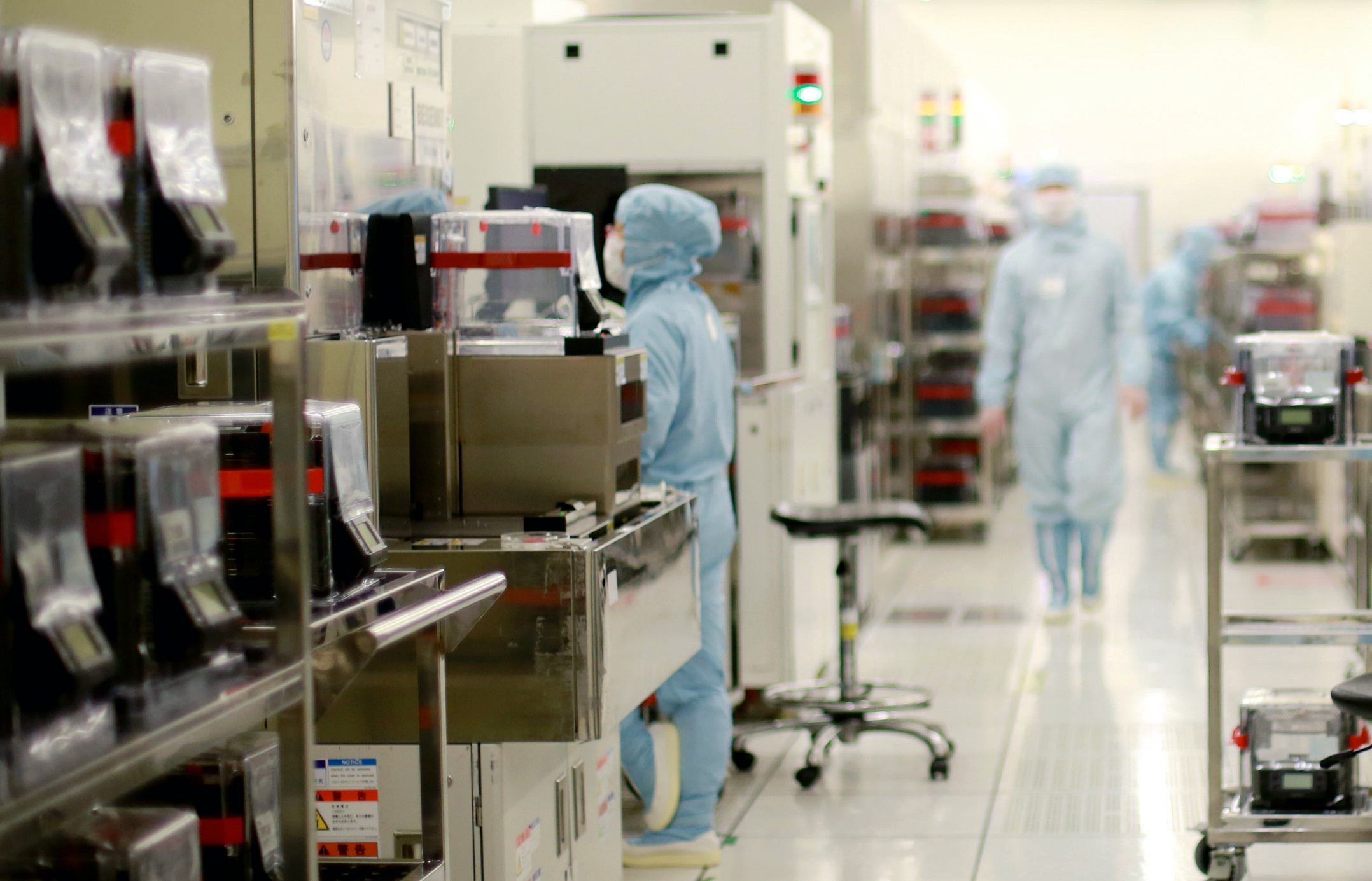
SMIC posted record full-year 2025 revenue of $9.33 billion, up 16.2% year-over-year, according to the company's annual results. Full-year utilization averaged 93.5%, a jump of eight percentage points from 2024, and wafer shipments rose 20.9% to roughly 9.7 million 8-inch-equivalent wafers.
Annual capex, meanwhile, ran at over $7 billion, reflecting an aggressive capacity build-out that is compressing margins: full-year gross margin was 21%, and the company guided Q4 2025 gross margin to 18% to 20% as depreciation from new fabs weighed on profitability even at near-full loading.
SMIC's production stack officially spans 350nm to 7nm, but the vast majority of output sits at 28nm and above. 28nm HKMG and PolySiON variants serve smartphones, networking, and DDICs. Nodes from 40nm through 180nm cover an alog, power management, RF, image sensors, and microcontrollers.
At the advanced end, SMIC's N+2 process (7nm-class) is in production for Huawei's Kirin 9000S, 9020, and Ascend 910C, with an estimated 20,000 WSPM of capacity. N+3, confirmed on the Huawei Kirin 9030 in December, extends 7nm-class scaling using DUV multi-patterning, though TechInsights characterized it as firmly 7nm/6nm-equivalent in absolute terms rather than a true 5nm node.
Swipe to scroll horizontally
Node
Technology
Key fabs
Status
N+3 (~7nm/6nm-class)
DUV multi-patterning; no EUV access
SN1/SN2, Shanghai
Limited production (Huawei)
N+2 (7nm-class)
DUV multi-patterning; ~20K WSPM; yields ~60-70%
SN1/SN2, Shanghai
Production
14nm FinFET
First-gen FinFET; folded into 28nm reporting since 2023
Shanghai
Production
28nm (HKMG/Poly)
Core expansion node
Shanghai (Lin-G ang); Shenzhen; Beijing
Production
40/55/65nm
Analog, power, RF
Multiple sites
Production
90-350nm
Legacy analog, MCUs, sensors
Multiple sites
Production
Four major new 12-inch fabs are under construction or recently completed, in Shanghai (Lin-Gang), Shenzhen, Beijing, and Tianjin, including an $8.87 billion facility, collectively targeting approximately 340,000 wafer starts per month of new 28nm-and-above capacity.
Export controls from the U.S., the Netherlands, Japan, and Taiwan constrain SMIC's ability to scale its advanced nodes. The company has been on the U.S. Entity List since December 2020, blocking access to ASML EUV scanners and progressively tightening DUV and etch equipment supply.
Taiwan added SMIC and Huawei to its own export-control blacklist in Ju ne 2025, requiring permits for high-tech equipment shipments. Although it was reported back in August that SMIC planned to double its 7nm capacity in 2026, the company remains constrained by tooling access: analysts estimate SMIC's advanced-node capacity will remain in the low tens of thousands of wafer starts per month rather than the hundreds of thousands that an unconstrained buildout would target.
SMIC's pricing reflects the competitive pressures in the mature-node segment, with the company having reportedly cut 28nm wafer prices by roughly 40% in early 2025, dropping from approximately $2,500 to $1,500 per wafer, before reversing course with a roughly 10% increase later in the year as utilization exceeded 95%.
Pricing and demand
After two years of price declines driven by Chinese capacity additions, the mature-node segment is reaching a floor. TrendFor ce reported in March that UMC, VIS, Powerchip, and Nexchip were preparing price increases of up to 10% from April through June this year, with the latter confirming a 10% hike effective from June.
One big factor is tightening supply alongside the cyclical recovery: TSMC has been reallocating 40-90nm production capacity toward CoWoS advanced packaging and silicon interposer fabrication for AI accelerators, reducing the available mature-node wafer supply from the world's largest foundry.
Demand from automotive (GloFo’s automotive revenue alone is on track for $1.5 billion in 2026), power management ICs for AI servers (typically manufactured on 28-55nm BCD processes), DDICs, and embedded flash microcontrollers continues to grow.
Swipe to scroll horizontally
Foundry
FY2025 revenue
Global share (TrendForce)
Most advanced production node
2026 capex
GlobalFoundries
$6.79 billion
3.87%
12LP FinFET
~15% to 20% of revenue
UMC
$7.63 billion
4.35%
14nm FinFET (12nm in development)
~$1.5 billion
SMIC
$9.33 billion
5.32%
N+2/N+3 (7nm-class, DUV)
$7 billion+
Whether these three foundries remain independent is an open question. The Project Ultron reports suggest that at least one party has considered consolidation, and the logic for doing so, at least in terms of economics, grows as margins compress and capex requirements grow.
While SMIC's expansion is state-backed and largely insulated from commercial return calculations, GloFo’s is tied to U.S. industrial policy and defense spending, and UMC's future hinges on whether 12nm FinFET with Intel can deliver the revenues that pure mature-node services cannot.

 eSIM Studios

No comments